
Advanced materials · Precision manufacturing
Build beyond
traditional manufacturing.
From material and forming to precision finishing and delivery, we turn complex designs into production-ready manufacturing routes.
One engineering interface. Multiple manufacturing routes.
We choose the process around the part—not the other way around.
Galaxy Star connects materials, additive manufacturing, precision forming, machining and quality resources through one engineering-led team.
Geometry, material, volume, critical dimensions and operating conditions determine the route—from prototype validation to repeatable production.

One platform.
Multiple paths to production.
We select and combine the right process for the geometry, material, performance and production volume of each project.
 01
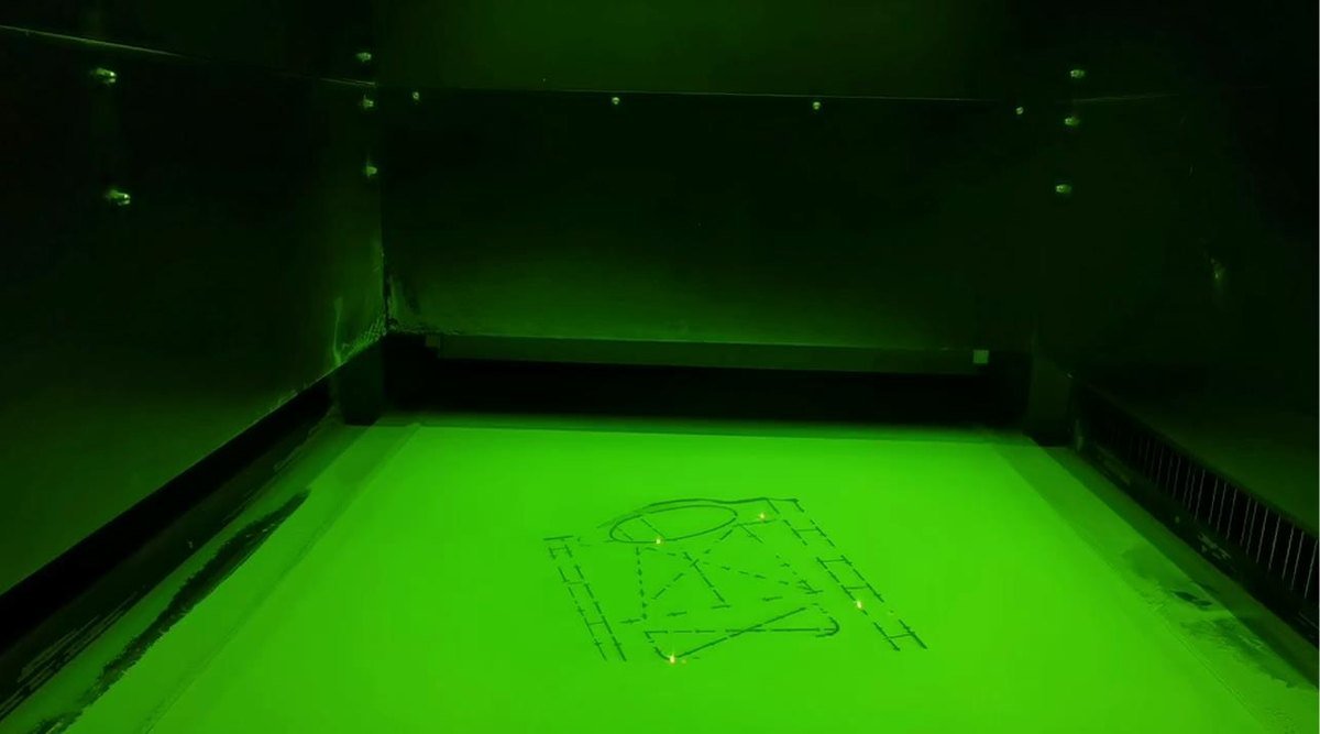
01Metal Additive Manufacturing
Complex channels, lightweight structures, rapid iteration and production-oriented metal printing.
Explore capability ↗ 02
02Precision Manufacturing
MIM, precision injection, tooling and CNC are combined for repeatable component production.
Explore capability ↗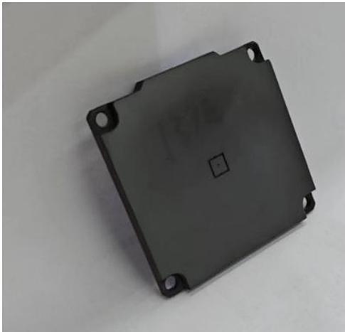 03
03Silicon Carbide
Silicon carbide components for low-expansion, high-rigidity, thermal and corrosive environments.
Explore capability ↗ 04
04Finishing & Quality
Machining, surface finishing, assembly and inspection complete the manufacturing route.
Explore capability ↗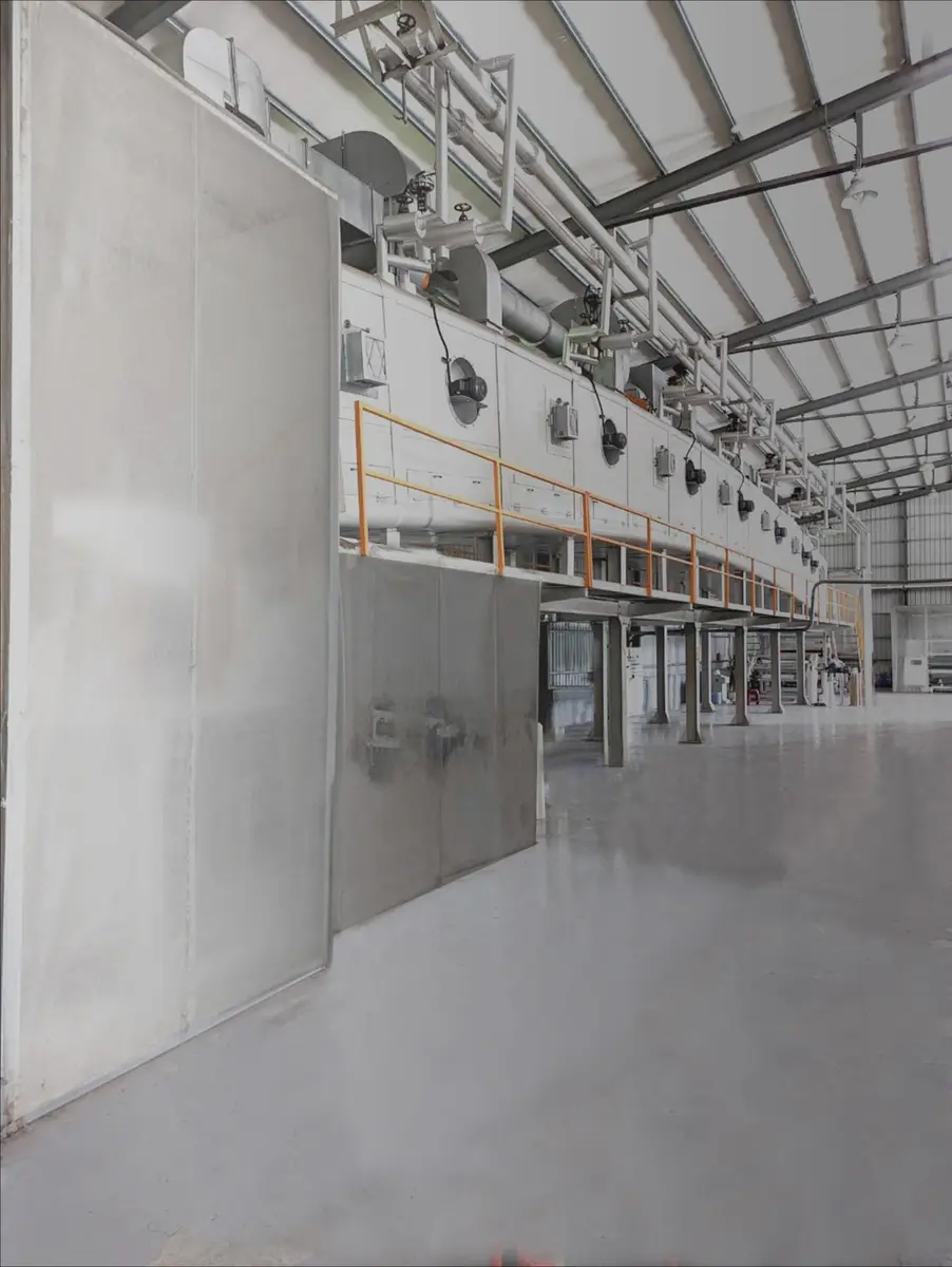 05
05Semiconductor Process & Packaging
Wafer-plating interfaces, adhesive formulation, precision coating, slitting and application-led verification.
Explore capability ↗Semiconductor
SiC structures, wafer-plating interfaces and carrier-tape packaging materials for process-specific requirements.
Wearables & electronics
Detailed metal components with repeatable geometry and controlled finishes.
Medical & automotive
Functional parts built around material, validation and production requirements.
Tooling & industrial
Conformal structures, functional tooling and parts for demanding equipment.
Manufacturing evidence,
shown at useful scale.
Selected applications demonstrate how our materials, processes and verification resources support real manufacturing requirements.
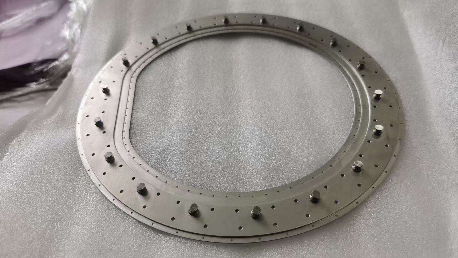
SEMICONDUCTORSilicon carbide precision structures ↗
Representative chucks, beams, mirrors and optical bases for demanding semiconductor and measurement environments.
 SEMICONDUCTOR PROCESS
CRS wafer-plating interface ↗
Six 6-inch wafer records document 99.65–99.99% AOI yield, 5.6–8.8 μm maximum coplanarity and no detected voids, with leakage-related loss retained for process review.
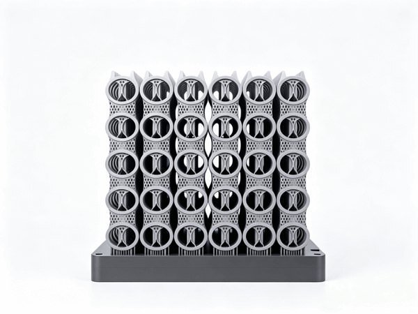 WEARABLES
Smart wearable components ↗
Production layouts for detailed metal parts, supported by finishing and inspection routes.
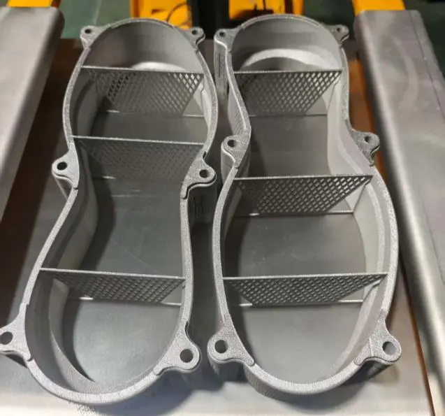 TOOLING
Metal additive shoe tooling ↗
Metal additive manufacturing consolidates the tooling route while enabling integrated lattice, venting and internal structures.
From challenge
to production.
A clear engineering path keeps technical decisions, validation and delivery aligned from the beginning.
Assess
Drawing, material, quantity, interfaces and operating conditions.
Select
Choose and connect the suitable forming, machining and finishing route.
Validate
Prototype, verify critical features and confirm repeatable process windows.
Produce
Scale manufacturing with inspection, documentation and delivery control.
Have a drawing, sample
or manufacturing requirement?
Share the material, estimated quantity, critical dimensions and operating conditions. We will help identify a practical route forward.
Start a project ↗