
SEMICONDUCTOR PROCESS & PACKAGING
Process interfaces and packaging materials, engineered around the application.
CRS wafer-plating interfaces and M6 heat-seal cover tape connect equipment compatibility, adhesive formulation, precision coating, slitting and verification in one application-led capability.
From wafer plating to carrier-tape packaging.
Galaxy Star connects equipment interfaces, functional adhesives, precision coating, slitting and verification through two application-specific product systems.
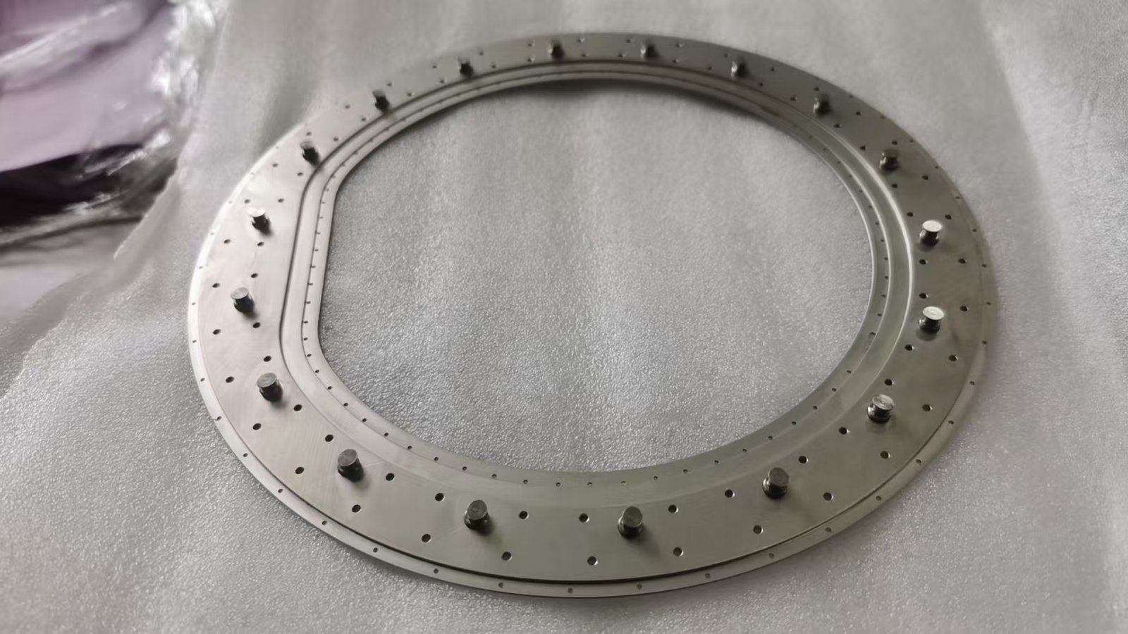
CRS conductive contact & seal
Conductive contact, liquid sealing and wafer positioning are integrated into one equipment interface. Dimensions and contact locations are configured around the wafer, fixture and protected area.
- 6 in
- Wafer process validation
- 2D + 3D
- AOI inspection
- 5.6–8.8 μm
- Coplanarity results
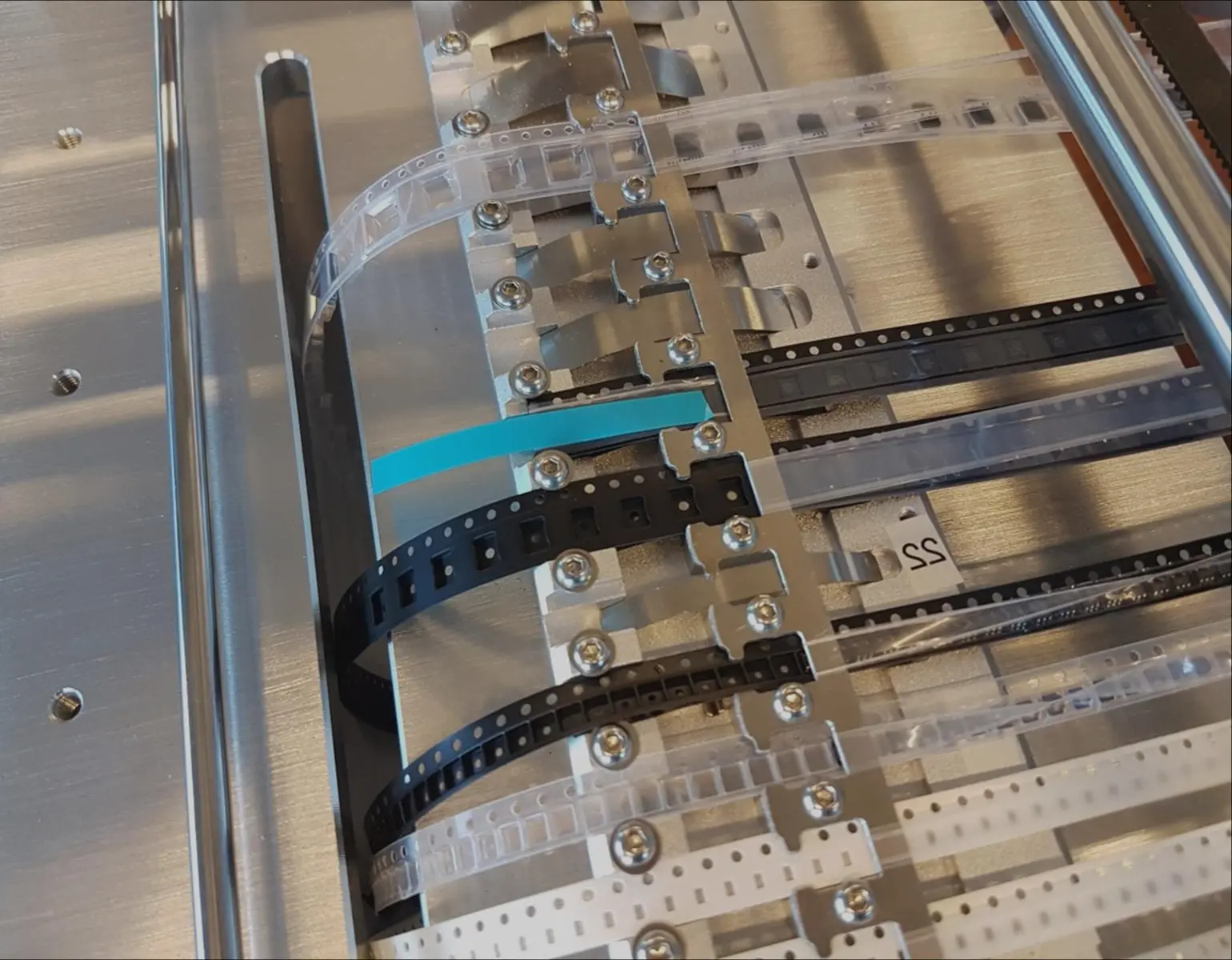
M6 antistatic heat-seal cover tape
A 43 μm multilayer cover tape combines PET, PE and heat-seal layers for stable sealing, peel behaviour, light transmission and physical antistatic performance.
- 43 μm
- Nominal thickness
- PS / PC / PET
- Carrier materials
- 720 h
- Ageing evaluation
Product performance begins with controlled process resources.
Real product and equipment photographs connect each capability to the manufacturing step it supports.
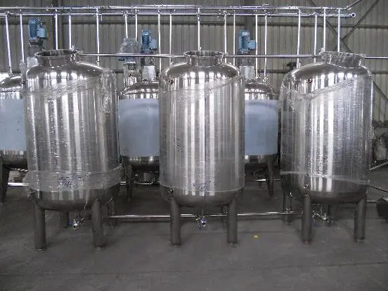
Adhesive formulation
Dedicated reaction vessels and controlled raw-material ranges support stable heat-seal adhesive formulation.
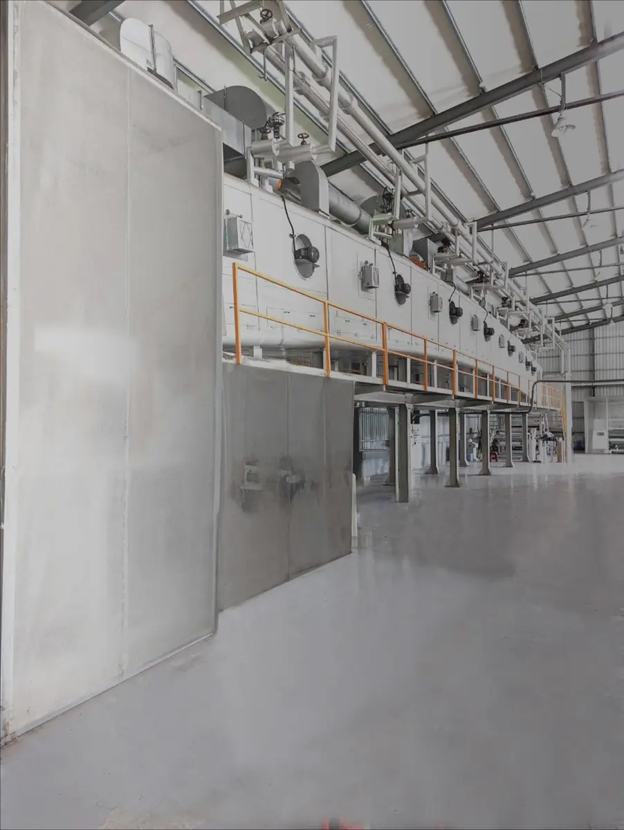
Precision coating
A 30-m multifunction coating line connects adhesive preparation, drying and precision thickness control.
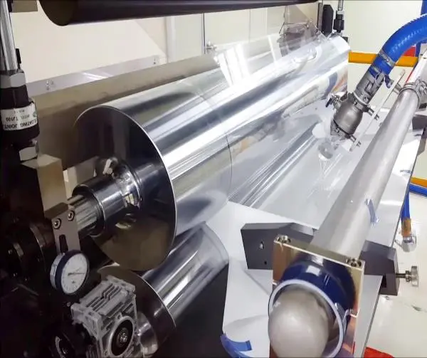
Precision slitting
Computer-controlled tension and precision tooling reduce edge lift, notches and dimensional variation.
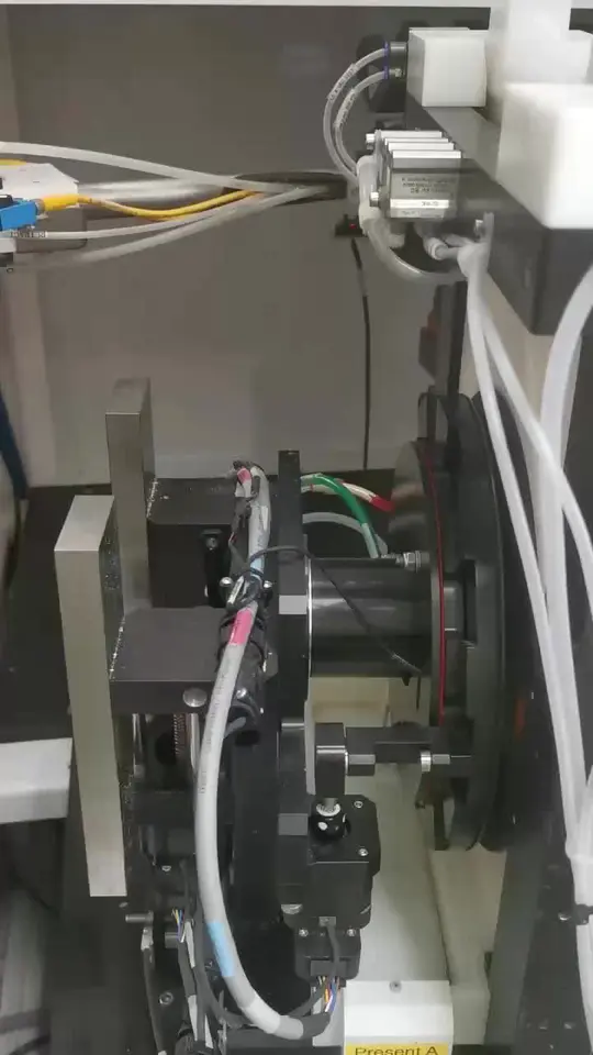
Equipment integration
Equipment, wafer geometry, contact position, sealing boundary and plating chemistry are reviewed as one interface.
Define the interface, verify the result, close the loop.
CRS and M6 are presented through their actual application conditions, process controls and release-verification route.
Conductive contact & isolation
CRS delivers current to the wafer while separating plating liquid from protected areas.
Wafer-level verification
Six-inch wafer records include 2D and 3D AOI, bump yield, height distribution, coplanarity and defect analysis.
Sealing & peel stability
M6 evaluations cover PS and PC carrier tapes across multiple sealing temperatures and ageing periods.
Release verification
Appearance, mechanical performance, light transmission, surface resistance, heat sealing and peel behaviour are checked before release.
START A PROJECT
Let’s manufacture what comes next.
Share your design, application or manufacturing challenge.
Talk to our team↗