
WAFER-PLATING INTERFACE ENGINEERING
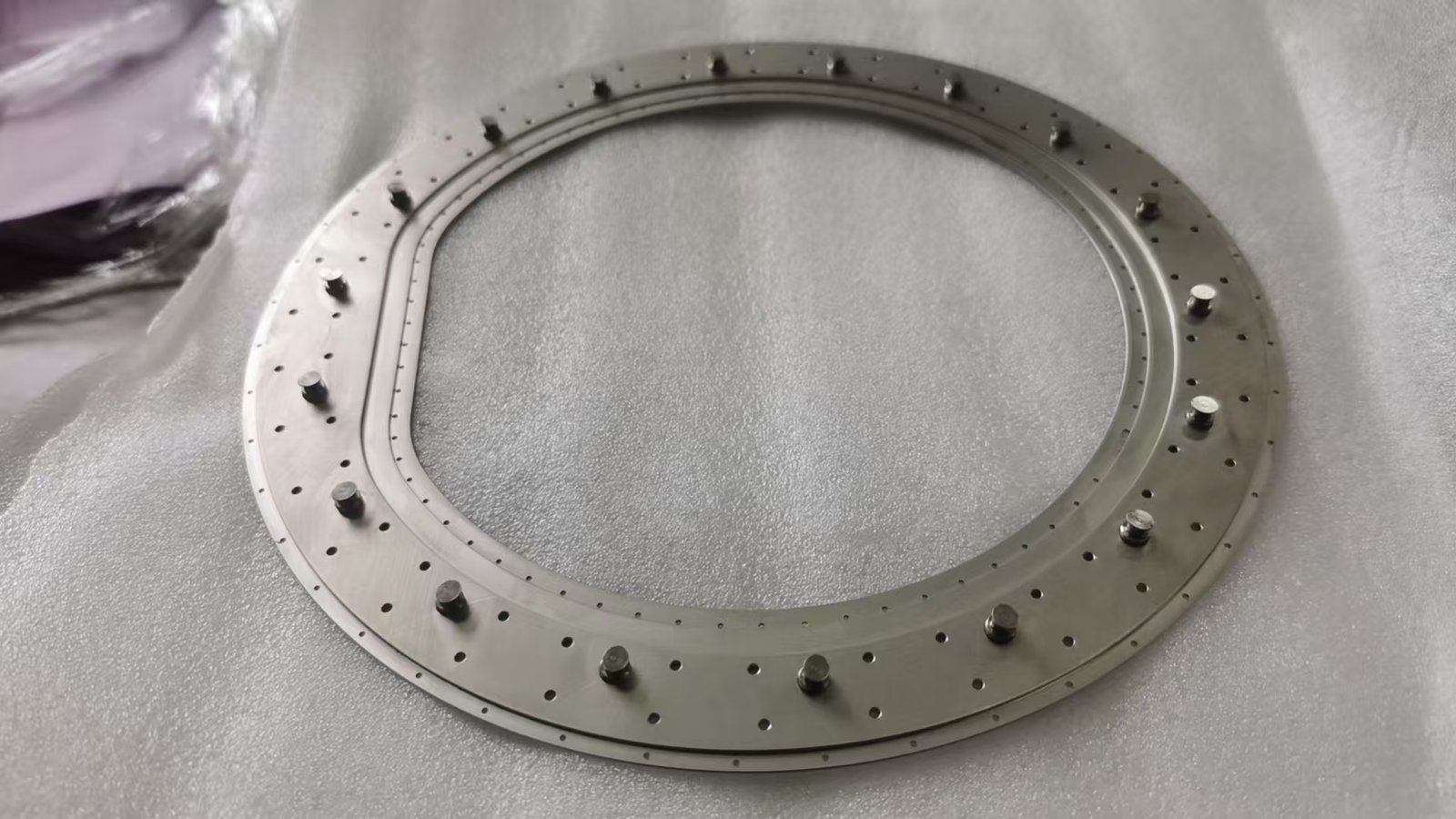
CRS conductive contact and sealing solution.
From equipment interfaces and wafer geometry to electrical contact, liquid sealing and process verification, we connect the critical conditions into one application-led solution.
01WHY GALAXY STAR
From interface conditions to measurable process results.
CRS projects connect equipment conditions, component design and wafer-level verification through one technical review route.
Interface-led engineering
We begin with wafer geometry, installation space and contact positions, then define the conductive and sealing interface around the real equipment conditions.
Contact and sealing together
Electrical contact, liquid isolation and stable positioning are reviewed as one connected interface instead of separate component requirements.
Verification closes the loop
AOI, coplanarity and defect review provide measurable feedback for interface conditions and process adjustments before release.
02PRODUCT & EQUIPMENT CONTEXT
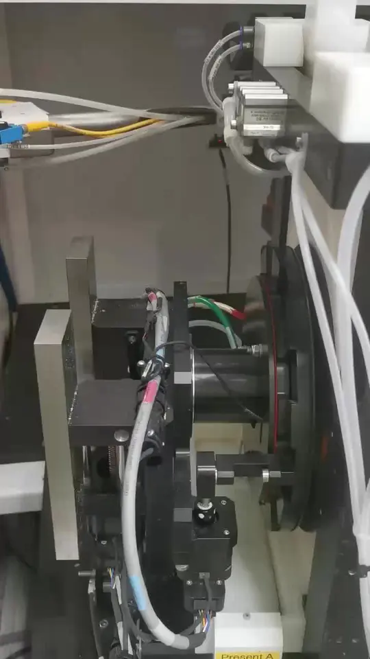
The interface, shown at the scale that matters.
03ENGINEERING & VALIDATION
Define, verify and refine the interface.
Conductive contact and sealing
The contact and sealing interface is designed to deliver current to the wafer while isolating plating liquid from protected areas.
Application-specific interface review
CRS specifications are reviewed against the equipment model, wafer size, installation geometry, contact position and process chemistry so the interface can be matched to the intended operating conditions.
Six-inch wafer process validation
Six wafer records were reviewed through 2D and 3D AOI, final bump yield, height distribution, coplanarity and defect analysis. AOI yield ranged from 99.65% to 99.99%; the recorded maximum coplanarity ranged from 5.6 to 8.8 μm, within the stated criterion below 10 μm; no voids were detected.
Defect review and process feedback
The evaluation also retained a leakage-related record with 69 two-dimensional losses. Rather than excluding the anomaly, it is used to review sealing conditions, equipment interfaces and operating parameters before production release.
Information required for assessment
Please provide the complete equipment model, wafer diameter, existing part number or photographs, dimensional drawings and plating chemistry before quotation.
START A PROJECT
Let’s manufacture what comes next.
Share your design, application or manufacturing challenge.
Talk to our team↗