
INDUSTRIES & OUTCOMES
Start with the industry. Prove it with the part.
Explore common manufacturing challenges, applicable capabilities and representative outcomes across six application fields.
Six fields. One application-led route.
Explore proven manufacturing routes and representative parts across semiconductor, wearable, medical, automotive, footwear and industrial applications.
Semiconductor
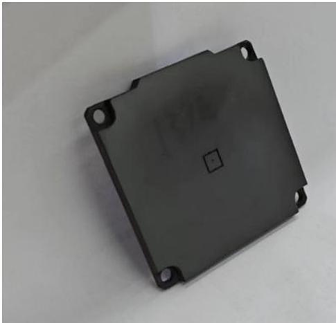
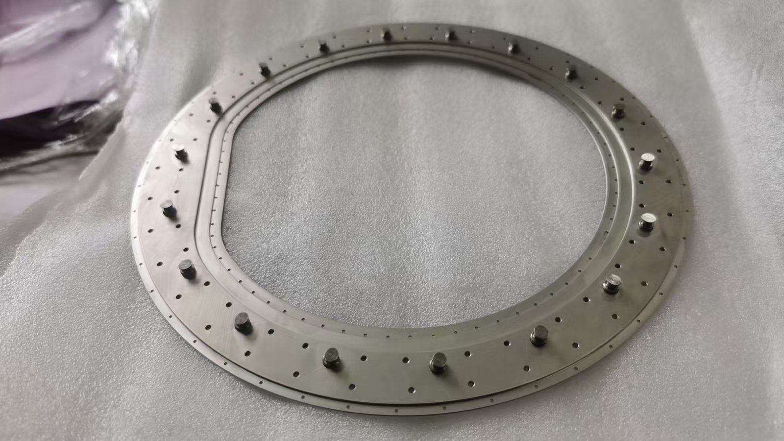
SiC structures, wafer-plating interfaces and carrier-tape packaging materials are selected around thermal, chemical, sealing and process-control requirements.
View related products ↗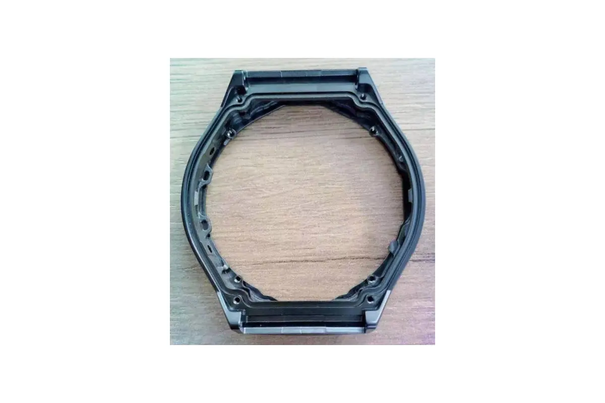
Wearables & consumer electronics
Fine geometry, compact structures, repeatable volume and controlled cosmetic finishes.
View related products ↗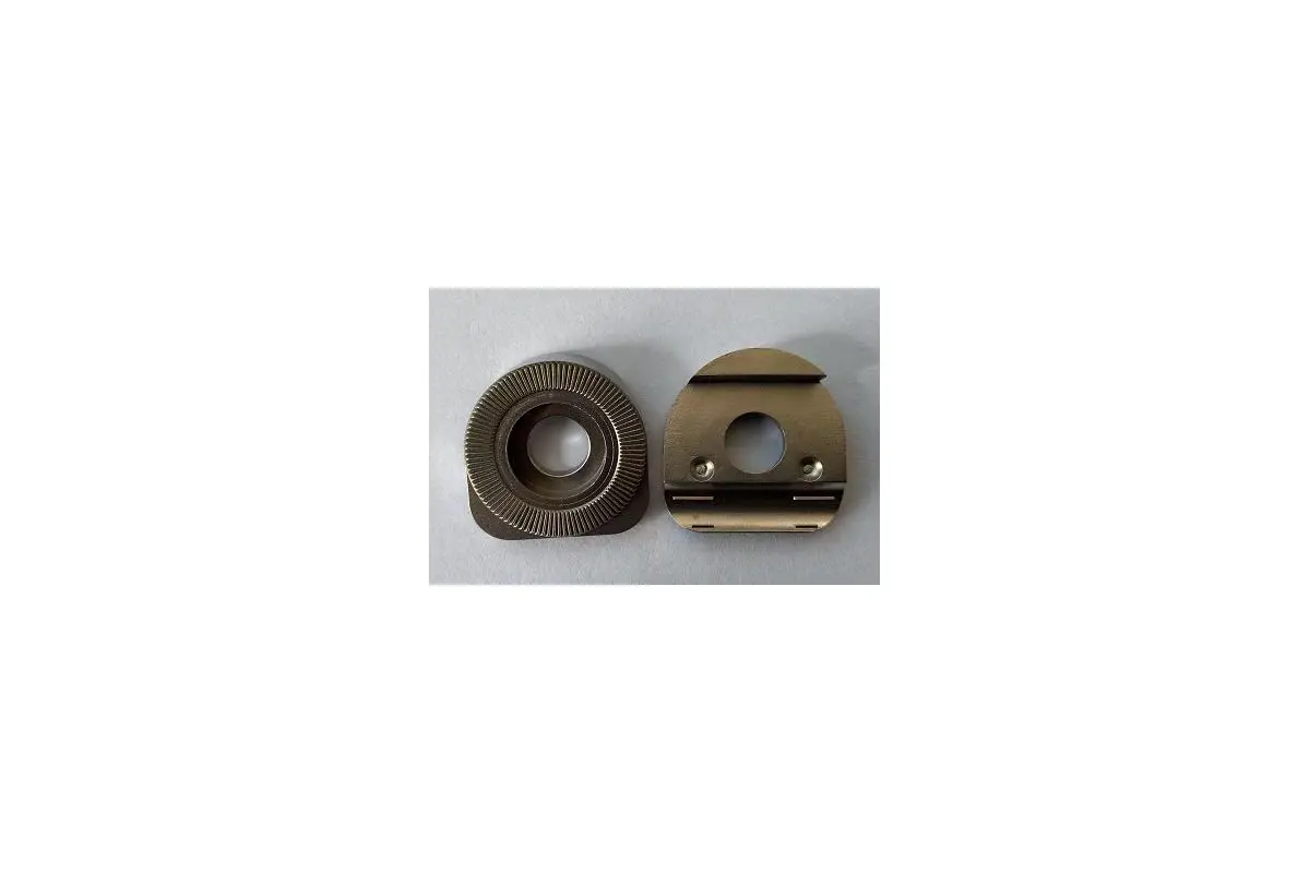
Medical devices
Material selection, small intricate parts and application-led validation.
View related products ↗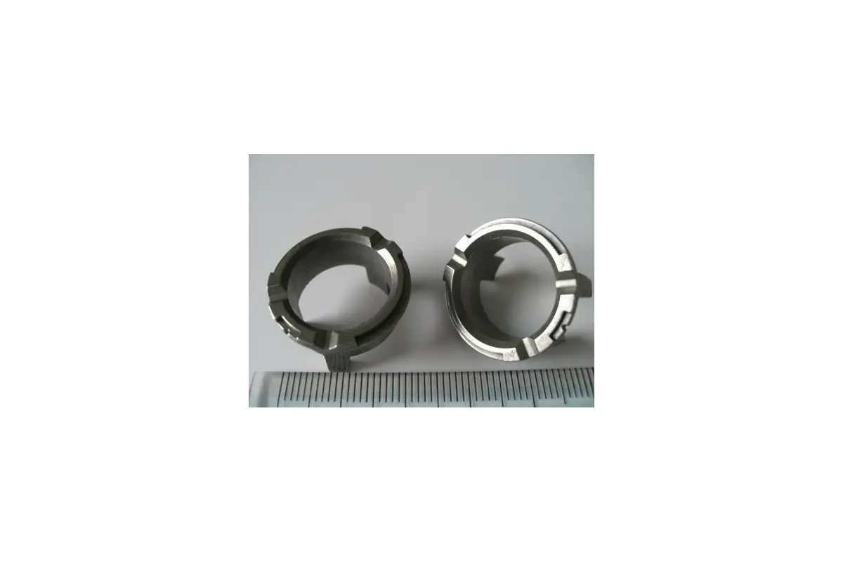
Automotive & transport
Durable functional parts, repeatable forming and production quality control.
View related products ↗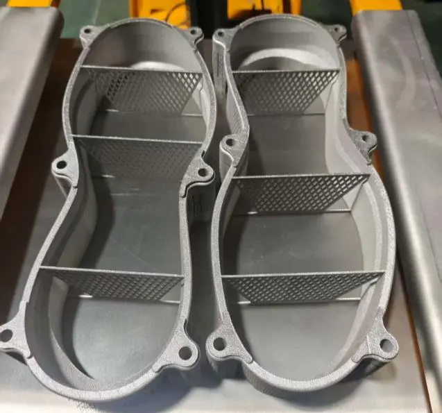
Footwear & tooling
Integrated lattice, venting and internal structures through a streamlined additive route.
View related products ↗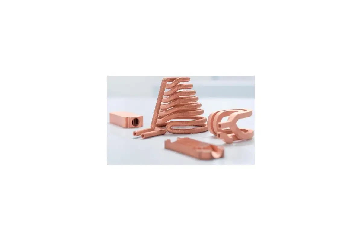
Industrial equipment
Complex channels, thermal structures and precision components for demanding systems.
View related products ↗Manufacturing outcomes built around real parts.
Representative production images connect each application to its material, process route and engineering value.
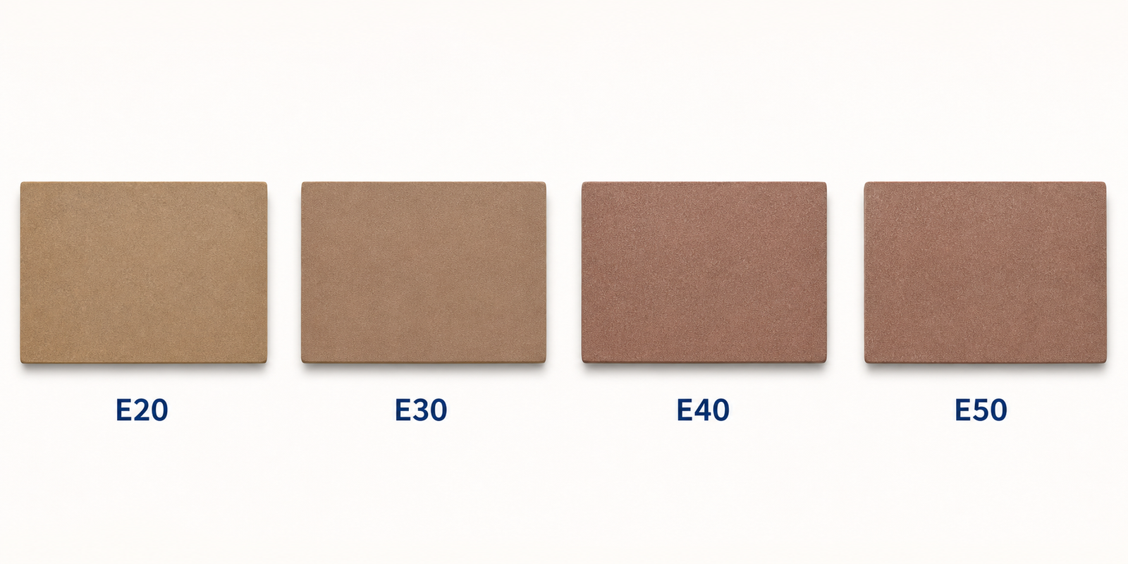
Semiconductor packaging validation
E40 wafer-dicing dressing boards completed a semiconductor-packaging customer’s purchasing-specification validation and entered application use, replacing approximately 70% of the referenced Japanese-brand volume.
Explore the manufacturing route ↗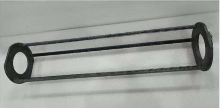
Semiconductor furnace hot-zone project
Horizontal SiC wafer boats and related hot-zone components support oxidation and diffusion environments near 1,250°C with oxygen, nitrogen and limited hydrogen chloride.
Explore the manufacturing route ↗Wafer-inspection optical baseplate
A lightweight SiC dual-optical-path baseplate provides high stiffness, low thermal expansion and geometric stability for wafer inspection equipment.
Explore the manufacturing route ↗
Wafer-inspection chuck deployment
Precision SiC chuck interfaces support 6-, 8- and 12-inch wafer inspection, combining mirror finishing with low mass and stable positioning.
Explore the manufacturing route ↗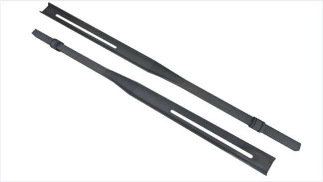
Semiconductor furnace paddle project
SiC cantilever paddles support stable wafer loading in high-temperature diffusion and oxidation furnaces, with geometry and interfaces configured for each furnace platform.
Explore the manufacturing route ↗START A PROJECT
Let’s manufacture what comes next.
Share your design, application or manufacturing challenge.
Talk to our team↗